Previous Progress
Custom CCD Driver Board
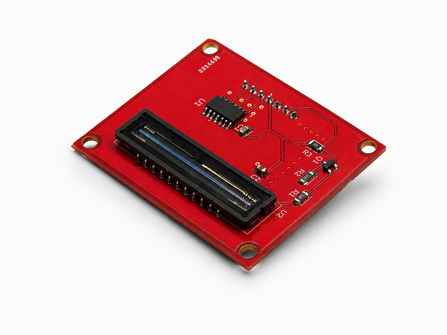
The team designed and assembled a custom printed circuit board to serve as the analog front end. This board manages the physical connection to the TCD1304DG linear CCD sensor. It performs DC offset adjustment to align the sensor output with the microcontroller voltage range. The circuit includes low pass filtering to remove high frequency noise before the signal reaches the analog to digital converter. We completed the schematic design and fabricated the board using surface mount components.
Embedded Data Acquisition
Extracting readable data from the CCD requires precise timing control. The firmware uses an STM32 microcontroller configured with three hardware timers to generate the exact clock pulses demanded by the sensor. As the sensor outputs pixel voltage levels the microcontroller samples the data using a 12 bit analog to digital converter. We implemented direct memory access to transfer this data continuously without burdening the primary processor. This architecture allows the system to build complete spectral frames in real time.
Desktop Software Interface
We developed a custom graphical user interface in Python to receive and display the spectral data. The software connects to the microcontroller over a USB serial connection to read the incoming frame buffers. It renders the raw pixel data into a live intensity graph for immediate visual feedback. The application includes features to record the spectral data to a file for later analysis. We also built the foundational code for mapping pixel indices to specific optical wavelengths.
Current Progress
Development of the Optical Calibration Device
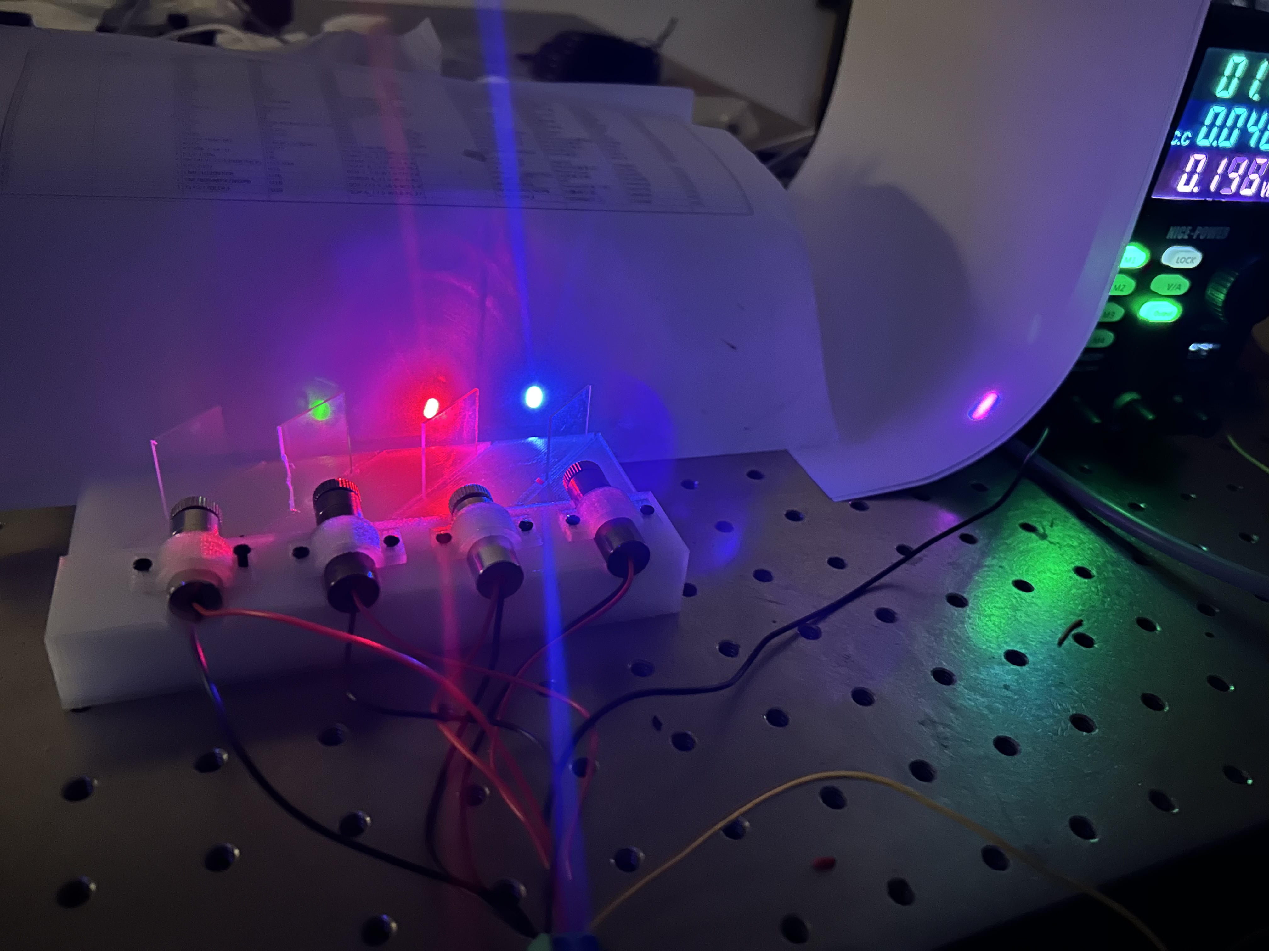
The team prioritized the development of a custom optical calibration device to ensure precise wavelength mapping. We engineered a 3D printed housing designed to securely hold laser diodes and alligned glass mirrors. Initial physical testing revealed clearance issues with the lenses. We quickly redesigned the fixture to incorporate expanded lens clearance and adjustable tilt mechanisms for the laser diodes. This redesign improves the alignment of the test LEDs and isolates the light to capture highly accurate baseline readings.
System Modeling and 3D Optix Simulations
Validating the optical path before final assembly requires highly accurate modeling. We evaluated multiple optical modeling programs and selected 3D Optix due to its streamlined interface and simple integration with standard optical components. We imported our specific diffraction grating parameters into the software to begin simulating the precise behavior of the light path. Current simulation efforts focus heavily on analyzing second order diffraction. This virtual environment allows us to optimize component placement and plan the final physical enclosure with complete confidence.
Hardware Integration and Data Acquisition
We successfully transitioned to direct optical bench testing and achieved our first live data acquisition. By connecting the CCD sensor and the microcontroller to an existing optical module, we captured live frame data and distinct light intensity peaks through our custom graphical user interface. We procured low OH multimode fiber optic cables and SMA mating sleeves because standard silica fibers absorb excessive light in the 800 to 1000 nanometer range. Our embedded systems architecture successfully reached the target 125 Hz frame rate. We are now isolating further embedded software improvements to triggering, integration time control, and background subtraction.